Solar Cells

A solar cell is, in principle, a simple semiconductor✶ device that converts light into electric energy. The conversion is accomplished by absorbing light and ionizing crystal atoms, thereby creating free, negatively charged electrons and positively charged ions. If these ions are created from the basic crystal atoms, then their ionized state can be exchanged readily to a neighbor from which it can be exchanged to another neighbor and so forth; that is, this ionized state is mobile; it behaves like an electron, and it is called a hole. It has properties similar to a free electron except that it has the opposite charge.
✶ Solar cells can be made from single crystals, crystalline and amorphous semiconductors. For simplicity this article begins with a description of crystalline material.
Each photon of the light that has a high enough energy to be absorbed by the crystal's atoms will set free an electron hole pair. The electron and hole are free to move through the lattice in a Brownian motion ; however, on average they will never move too far from each other. When the electron comes too close to a hole during their Brownian motion, they will recombine. On the other hand, when they experience an electric field, this will tend to separate the electrons from the holes; the electrons will drift toward the positive pole (the anode), and the positively charged holes will drift toward the cathode. Recombination will then take place in the external circuit (within the electric wires). Consequently a current will flow. Since it is generated by photons, one speaks of a photo current. And the semiconductor that performs this effect is called a photo conductor. Photo conductors are passive devices. They react to light by changing their electric conductivity. In order to activate them an external electric power source, such as a battery, needs to be supplied to draw a current that increases with increasing light intensity. There are many photo conductor devices in our surroundings; as for example, in cameras, in streetlight controls to switch the lights off at dawn and on at dusk, or for light barriers in garage door safety controls.
However, if an electric field is incorporated into the semiconductor, it will separate the electrons and holes. The part of the crystal that accumulates the electrons will be negatively charged; the part that accumulates the holes will be positively charged. The resulting potential difference, referred to as an open circuit, can be picked up by an electrometer. When electrodes are provided at both sides, a current can flow between them. The crystal, when exposed to sunlight, acts as a battery and becomes a solar cell (see Figure 1).
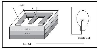
Such a built-in field is easily created in certain semiconductors that can dissolve a small quantity of different impurities; can donate a free electron, called a donor; and can also accept an additional electron, called an acceptor. When dissolving these impurities (called doping) separately in different parts of the crystal, the region that contains donors is called the n -type region, the region with acceptors is called the p -type region. Between these two regions lies an np junction. This region represents the built-in field, since the n -type region is negatively charged compared to the p -type region. Here electrons that are created by light can be separated from the accompanying holes, with the electrons moving into the attracting p -type region and the holes moving preferably into the n -type region.
This, in principle, describes the essentials of a solar cell. The following portions of the article deal with each part of the solar cell in more detail, present a quantitative description of its performance, indicate performance limitations (called the "efficiency" of the solar cell), and give a variety of solar cell materials with comparative performance.
The pn Junction
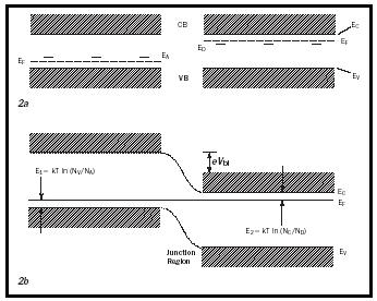
The pn -junction can be easily understood in the band model with the conduction band populated by free electrons and the valence band populated by free holes. Without light, these carriers are created in thermodynamic equilibrium by donors and acceptors respectively. Mathematically their concentration is given by the Fermi-function (Eq.1)
(1)
with the determining Fermi level E F , in the n -type region lying essentially in the middle between the donor level and the lower edge of the conduction band, E c . N c is the effective density of states at the lower edge of the conduction band and is on the order of 10 19 cm −3 . A similar equation holds for the density of holes; here the Fermi level lies between the acceptor level and the upper edge of the valence band (see Figure 2a).
In thermodynamic equilibrium the Fermi level is horizontal throughout the crystal, thereby forcing both conduction and valence bands to bend, creating the pn -junction (see Figure 2b). Electrons from the p -type region will thereby "roll down" the hill and holes from the n -type region will "bubble up" the slope; hence both will be separated until their charge will force a reduction potential barrier so that the thermal motion across the junction will become equal from the left and from the right.
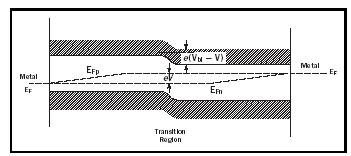
With light, additional carriers are created, hence equation 1 needs to be modified, replacing E F with E Fn or E Fp , the two quasi-Fermi levels in the n -type or p -type region respectively. These quasi-Fermi levels are now split; the higher the light intensity the more they split. Close to the electrode both quasi-Fermi levels collapse toward the majority quasi-Fermi level, where they are connected to the metal Fermi level (Figure 3). This shift of the Fermi levels in the electrodes represents the open circuit voltage that can be approximated by the shift of the minority quasi-Fermi levels (Figure 3):
V oc ≈ E Fn ( p ) – E Fp ( n ) (2)
Current-Voltage Characteristics
Materials with a pn -junction show a nonlinear, rectifying characteristic, since it is much easier to move electrons from the electrode through the p -type region and through the junction than from the n -type region over the junction barrier into the p -type region. The current-voltage characteristic through a pn -junction is given by the typical diode equation:
(3)
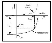
as shown as the dark current curve in Figure 4.
When the device is exposed to light, the additional carriers cause an increased current, recognized by an essentially parallel shift of the characteristic downward by j L , shown in Figure 4. (For a more precise discussion see Böer, 2002.)
The photovoltaic characteristic is consequently given by (see, e.g., Fahrenbruch and Bube 1983):
(4)
j L is the maximum current obtained in short-circuiting the device. With j 0 << j L ∼ j SC one obtains for the open circuit voltage (when j = 0) from Eq. 4:
(5)
Whenever the current-voltage characteristic extends into the fourth quadrant, electric power can be extracted. Its maximum value is given by the largest rectangle that can be inscribed in the characteristic (Figure 4). This identifies the maximum power current, j mp and the maximum power voltage V mp . The ratio of the products of these maximum power points to the products of the short circuit current and open circuit voltage is called the fill factor, which can be approximated for ideal solar cells by (see, e.g., Green 2001):
(6)
with ν oc = V oc /( kT / e ). The actual fill factor is usually somewhat smaller and is a measure of the quality of the solar cell. It is a function of the diode doping and of solar cell materials.
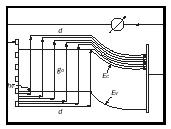
The net carrier transport in a solar cell can be pictured as shown in figure 5, with light ( hν ) coming from the left and generating (g 0 ) electron hole pairs in the p -type front layer (of thickness d ). The electrons move towards and through the junction, the holes in opposite direction. When both are shown as electron current (the arrow head is inverted for holes) one visualizes the continuity of the carrier flow and its building up with increasing depth of the front layer.
Solar Cell Materials
A wide variety of materials have the potential of yielding solar cells; several are considered attractive candidates for reasons of high conversion efficiency and ease of fabrication.
For a solar cell one can select a single semiconductor having a junction, usually referred to as homojunction, or a combination of two materials, with the junction at the interface referred to as heterojunction. The selected material needs to match the solar spectrum; i.e., it has to absorb most of the spectrum for maximizing the short circuit output, therefore it has to have a low band gap. However, this is counteracted by the desire to also have a large open circuit voltage, requiring a larger band gap and forcing a compromise. Consequently, for homojunction materials a band gap between 1 and 1.5 eV is preferred.
Typical representatives of this class of homojunction semiconductors are Si; several III-V compounds, most prominently GaAs; and from the class of II-VI compounds CdTe, since it can be doped p - and n -type, while others cannot. Several ternary compounds are also used, most prominently CuInSe 2 and similar ternaries. An example for a heterojunction cell is the CdS/CdTe combination (Meyers and Birkmire, 1995). For more details see Green (2001).
These materials can be employed as single crystals (Si and GaAs), as polycrystals (Si), other thin-film materials (CdTe and all ternaries), and as amorphous material (a-Si:H). Single crystals have the advantage of having high crystal quality and a minimum density of recombination centers; therefore they have a high carrier lifetime that is essential for the carriers to reach the junction after generation, in order to be separated and to contribute to the current.
Other factors that influence the output of solar cells are degradation of surfaces and of electrodes; the first causes a reduction of carrier lifetime, the second causes a reduction in solar cell life expectancies. An example of the first is the beneficial effect of a natural oxide layer that reduces surface recombination of Si solar cells, while special efforts need to be made for GaAs cells to passivate the surface. An example for the second effect is the CdTe solar cell, which has difficulties maintaining stable electrodes on the p -type side.
Optimization of Photon Absorption
In order to make maximum use of the impinging photons and obtain maximum solar cell output, one has to maximize surface penetration, minimize reflection, and reduce obstacles, such as electrodes.
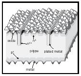
A typical example for such optimization is the structure (shown in Figure 6) developed by Martin Green and his group in order to produce highly-efficient Si solar cells. In addition to an anti-reflecting coating, it contains an etched pyramidical surface that permits light capture (velvet effect) by multiple reflections downward. It also reduces the surface cover of electrodes that are of sufficient thickness to carry the current by depositing it vertically into narrow grooves. It also minimizes the probability of both types of carriers reaching the same electrode by providing a repulsive field through strong doping of a thin surface layer.
Solar Cell Efficiency
Solar cell efficiency is a most valuable measure of its performance. With sunlight impinging from the zenith on a sunny day, a surface perpendicular to the light receives about 1 kW/m 2 . When converted by a solar cell of 10 percent efficiency (presently reached or exceeded by most commercially available solar panels), this means that 100 W/m 2 in electrical energy can be harvested. This is sufficient if surface areas are ample and the panels are relatively inexpensive. However, where surface areas are at a premium—e.g., on top of a solar car or in some satellites—it is essential to use more efficient solar cells. These are available from carefully engineered Si cells or from GaAs, reaching efficiencies close to 25 percent.
![Figure 7. Monolytic GaInP/GaAs solar space cell (panel a) and a similar AIGaAs/GaAs solar cell have reached 27.6% efficiency at AM 1.5 insolation (after Chung et al., 1990). [AM refers to the airmass, and AM 1.5 indicates a solar angle at which the light penetrates through 1.5 times the vertical thickness of the air, that is at a zenith angle of 48.19°.]](../images/chfa_04_img0855.jpg)
When still higher efficiencies are desired, one can resort to tandem solar cells made by adding a semiconductor of a lower band gap on the bottom, so that photons of lower energy that were not absorbed in the top cell have a second chance to be absorbed and produce additional electric power. Adding a third layer to such a tandem can be beneficial. An example is shown in Figure 7 for a monolytic cell (with matched current and only two electrodes). AlGaAs/GaAs tandem cells reach 27.8 percent efficiency. Mechanically stacked cells (with four electrodes) between GaAs and Si have reached 31 percent (Gee and Virshup, 1988). For more on a large variety of solar cell materials and their best efficiencies, see Green (2001) or Bube (1998). Comprehensive solar cell efficiency tables are provided in Green et al. (2000).
SEE ALSO Solid-State Devices .
Karl W. Böer
Bibliography
Böer, K. W. (2002). Survey of Semiconductor Physics, Vol. II. New York: John Wiley.
Bube, R. H. (1998). Photovoltaic Materials. London: Imperial College Press.
Chung, B. C; Virshup, G. F.; and Schultz, J. C. (2000). Proceedings of the 21st IEEE Photovolt. Spec. Conf . Kissimee, FL, p. 179.
Fahrenbruch, A. L., and Bube, R. H. (1983). Fundamentals in Solar Cells. New York: Academic Press.
Gee, J. M.; and Virshup, G. F. (1988). Proceedings of the 20th IEEE Photovol. Spec. Conf . Las Vegas, NV, p. 754.
Green, M. A. (2001). Solar Energy, the State of the Art. London: James & James.
Green, M. A.; Emery, K.; Bucher, K.; King, K. L.; and Igari, S. (2000). "Solar Cell Efficiency Tables." Progress in Photovoltaics 8: 377.
Meyers, V., and Birkmire, R. W. (1995). Progress in Photovoltaics 3: 393.
Comment about this article, ask questions, or add new information about this topic: