Surface Chemistry
Wolfgang Pauli once stated that "the surface was invented by the devil," illustrating the complexity and difficulty of studying the surfaces of materials. This prompts a fundamental question: What is the surface of a material? The simplest definition is that the surface is the boundary at which the atoms that make up one material terminate and interface with the atoms of a new material. If the surface is considered to be just the outermost layer of atoms of a material, then it comprises on average only 10 15 atoms per square centimeter (1 square centimeter equals 0.155 square inch), as compared to the bulk of the material, which consists of approximately 10 23 atoms per cubic centimeter. Surface chemistry is important in many critical chemical processes, such as enzymatic reactions at biological interfaces found in cell walls and membranes, in electronics at the surfaces and interfaces of microchips used in computers, and the heterogeneous catalysts found in the catalytic converter used for cleaning emissions in automobile exhausts.
The development of modern surface chemistry did not begin until the early 1960s as the tools needed to detect the small numbers of surface atoms relative to the bulk atoms (predominately through electron-based spectroscopies) became available. Almost thirty years later, the study of surface chemistry received another boost with the development of a new class of tools called scanned probe microscopies, which provide the ability to view the chemical changes of surfaces under different environmental conditions. Such tools were the first to allow for the direct three-dimensional mapping of positions of atoms at surfaces. These techniques changed the view of surfaces by offering scientists and engineers the ability to directly examine and modify surface chemistries at the atomic and molecular levels.
Seeing Is Believing: The Scanning Tunneling Microscope
In 1981 the first direct visualization of surface atoms was made using a new tool, the Scanning Tunneling Microscope (STM). This tool and the offshoots of its development, including the Atomic Force Microscope (AFM) and Near-field Scanning Optical Microscope (NSOM) have revolutionized the field of surface chemistry. For the first time many processes that occurred at surfaces and interfaces, such as catalytic reactions, could be directly probed. This revolution was so important that the inventors, German physicist Gerd Binnig and Swiss physicist Heinrich Rohrer, received the Nobel Prize in physics only five years later in 1986.
TUNNELING
Tunneling is the process in which electrons can pass from one metal to another, even though they are not in contact. This process occurs by coupling of the electronic states between the two surfaces.
The STM utilizes the quantum mechanical phenomenon of tunneling to visualize the positions of atoms on surfaces. A sharp metal tip is attached to a piezoelectric translator, which can position the tip with angstrom (1 Å = 1 × 10 −10 meters) precision. As the tip is scanned over the surface, electrons move between the tip and sample and a tunneling current is produced. This current is very sensitive to (i.e., exponentially dependent upon) the
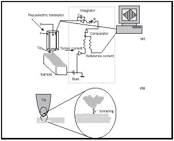
distance between the tip and sample. By attempting to maintain a constant current using a feedback loop monitored by a computer, the piezoelectric receives a signal from the computer to raise or lower the tip as it scans over the surface (Figure 1). Plotting the changes in tip height and position produces a three-dimensional image of the surface, yielding the ability to view the locations of single atoms and to manipulate their atomic positions.
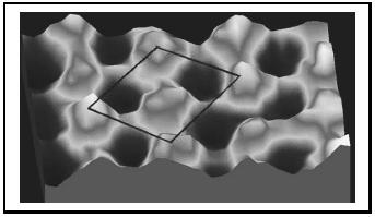
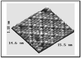
Numerous areas of research have benefited from this technique, including semiconductor technology, growth of metals, and heterogeneous catalysis. Shown in Figure 2 is an atomic resolution image of sulfur atoms on a rhodium surface. Because of the crystalline nature of the Rh surface, the S atoms position themselves in an ordered arrangement as they bond to the metal. Similarly, for surfaces such as silicon, the atomic positions can be viewed. STM revealed for the first time the organization of the structure of atoms on silicon surfaces, having a significant impact on the design of semi-conductor devices. Shown in Figure 3 is an image of the Si(111)−(7 × 7) restructured surface as viewed by STM. Imaging of semiconductors such as Si as a function of voltage between the tip and sample allows for direct visualization of the occupied and unoccupied states, a direct view into the chemistry of the surface atoms.
Seeing the Rest of the World: Atomic Force Microscopy
While STM gave researchers the ability to probe atomic scale events at metal and semiconducting surfaces, many of the materials of interest to surface scientists fall outside these classes of materials, such as the surfaces of oxides and biological materials that lack conductivity. AFM is a tool that provides similar surface mapping of materials as STM, but can be used for systems that are nonconductive as well.
PIEZOELECTRIC
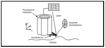
A piezoelectric is a ceramic material (typically a mixture of Pb, Zr, Ti, and O) that changes size with applied voltage. Quartz is an example of a naturally occurring piezoelectric. Piezoelectric materials are used to control the tip position in scanned probe microscopes because the changes in the piezoelectric dimensions can be controlled with sub-angstrom precision.
In AFM, a sharp tip on a cantilever is placed in contact with a surface. The forces acting between the tip and surface cause the cantilever to bend. Using a feedback loop, this force is held fixed as the tip is scanned and "feels" its way over the surface, producing an image of the surface topography (Figure 4). AFM measurements can be made in air or under liquids, which allows imaging of biologically important molecules and surfaces, within the nanoscale regime, under natural physiological conditions. AFM has also become an important tool in the measurement of surface properties ranging from basic structure to nanoscale mechanical properties such as friction, adhesion, and elasticity. The details of friction and adhesion are crucial at the nanoscale level, especially with the drive to move technology to even smaller length scales, leading to the development of microelectromechanical systems (MEMS) devices such as microscale motors, actuators, and switches. MEMS devices are currently used in critically important technologies such
as shock sensors for the deployment of airbags in automobiles. The surfaces of these devices are typically covered with silicon dioxide (glass); controlling the surface chemistry is essential in order to ensure the successful operation of the device.
Studies of adhesion by AFM have led the way to probing local chemical forces at surfaces allowing for the fundamental molecular forces between molecules to be measured directly. Other unique aspects of surface chemistry that AFM has been used to explore include the imaging of liquid surfaces. Modification of the AFM tip with metals allows for the local electric field between the tip and sample to be monitored. Changes in the dielectric properties such as the large contrast between water and many solid surfaces allow for the position of liquid droplets to be observed and for the structures of thin films of water to be probed. Due to the ubiquitous nature of water, the details of the surface chemistry of water are of key concern in a wide range of systems including the chemistry occurring in the stratosphere where ozone-depleting chemical reactions occur on ice surfaces.
Squeezing Light: Near-field Scanning Optical Microscopy
The images that are generated by STM and AFM show structure but no true chemical composition. The details of the local chemistry on surfaces at the nanoscale level, however, are very important to understanding surface properties. Optical spectroscopy and microscopy provide a means of chemically identifying materials; in conventional microscopy, however, the resolution limit is approximately half the wavelength of the light used to illuminate the sample. Thus, spatial resolutions are typically limited to approximately 200 nanometers (7.9 × 10 −6 inches) in the visible and approximately 5,000 nenometers (2.0 × 10 −4 inches) in the infrared parts of the electromagnetic spectrum.
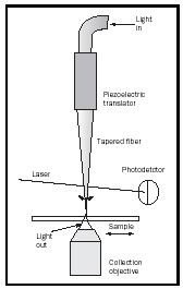
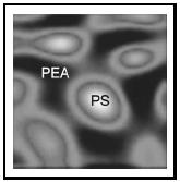
Near-field Scanning Optical Microscopy (NSOM) overcomes these limitations by "squeezing" the light through an aperture of approximately 50 nanometers (2.0 × 10 −6 inches), typically using a tapered optical fiber just as is used in most telecommunications signal transmissions. By bringing the tapered fiber to within about 10 nanometers (3.9 × 10 −7 inches) of a surface, the photons see only the local region of the surface where the tip is positioned (Figure 5). When the light is transmitted through the sample it is collected with a conventional microscope objective, spectroscopic as well as structural images of the materials on a surface can be observed. This approach has paved the way for single molecule spectroscopy and is opening new possibilities for the analysis of material properties at the nanometer scale. Technology is advancing into the infrared and microwave regions of the spectrum, allowing for the chemical composition and dielectric properties of materials to be probed with high spatial resolution. Figure 6 shows a near-field optical image of a polymer blend of polystyrene and polyethylacrylate, taken in the infrared region of the spectrum showing high spatial resolution spectroscopy.
Nanostructures on Surfaces
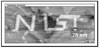
The design of nanostructures on surfaces using scanned probe microscopies enables the custom design and manipulation of matter on the atomic and molecular level. An STM or AFM tip can be used as a "nanowriter," placing and pushing around atoms and molecules on surfaces to make organized structures. Single atom positioning heralded by American physicist Donald Eigler at IBM showed the way in which atoms could be placed in complex structures using an STM to carry and position atoms on a surface with high precision. In 1987, using xenon atoms deposited on a nickel surface, researchers at IBM used the STM to write "I," "B," and "M" on a surface (Figure 7). Given the ability to write structures at this length scale, the entire Library of Congress could be written on the head of a pin. Although the timescale needed to write structures atom-by-atom makes this prohibitive as a general tool for large-scale lithography, the feasibility has been shown. This burgeoning area of nanotechnology has surface chemistry at its heart, as the detailed control of matter at the molecular level on surfaces is viewed as part of the next technological revolution.
The generation of nanostructures with AFM using dip-pen and nanografting patterning methods has shown great utility in the writing of complex molecules onto surfaces for use in nanoscale devices and sensors.
In dip-pen lithography an AFM tip "inked" with molecules is scanned along a surface in a controlled pattern. Under the appropriate conditions the molecules transfer from the tip to the surface, much as a fountain pen writes on a piece of paper.
Nanografting provides another means by which structures may be prepared on surfaces. In nanografting, a background layer of alkanethiols on gold is initially formed as a support matrix. When this surface is imaged in a background solution of a different molecule than the matrix, as the AFM tip scans through the matrix molecules, they are scraped away (mechanically removed) and replaced by the new molecules present in solution (Figure 8). This methodology has been successful in creating structures ranging from a few nanometers to tens of nanometers in dimension. Both of these approaches (and modifications thereof) are rapidly advancing the methodology of "nanowriting."
Bibliography
Binnig, G., and Rohrer, H. (1985). "The Scanning Tunneling Microscope." Scientific American 253: 50.
Bonnell, D., ed. (2001). Scanning Probe Microscopy and Spectroscopy: Theory, Techniques and Applications. Weinheim, Germany: Wiley-VCH.
Eigler, D. M., and Schweizer, E. K. (1990). "Positioning Single Atoms with a Scanning Tunneling Microscope." Nature 344: 524.
Hsu, S. M., and Ying, Z. C., eds. (2003). Nanotribology: Critical Assessment and Research Needs. Dordrecht, The Netherlands: Kluwer Academic.
Hu, J.; Xiao, X.; Ogletree, D. F.; and Salmeron, M. (1995). "Imaging the Condensation and Evaporation of Molecularly Thin Films of Water with Nanometer Resolution." Science 268: 267.
Liu, G.; Qian, Y.; and Xu, S. (2000). "Nanofabrication of Self-Assembled Monolayers Using Scanning Probe Lithography." Accounts of Chemical Research 33: 457.
Paesler, M. A., and Moyer, R. J., eds. (1996). Near-Field Optics: Theory, Instrumentation and Applications. Hoboken, NJ: Wiley.
Piner, R. D.; Zhu, J.; Xu, F.; Hong, S.; and Mirkin, C. A. (1999). "'Dip-Pen' Nano-lithography." Science 283: 661.
Somorjai, Gabor A. (1995). Introduction to Surface Chemistry. New York: Academic Press.
Zangwill, Andrew (1988). Physics at Surfaces. Cambridge, UK: Cambridge University Press.
Internet Resources
IBM Almaden Research Center Visualization Lab. "Moving Atoms." The IBM STM Image Gallery. Available from http://www.almaden.ibm.com/vis/stm/gallery.html .
Comment about this article, ask questions, or add new information about this topic: