Solid-State Devices
Solid-state devices are the controlling components of both high-tech and very ordinary devices. Their widespread usage is related to the fact that they can be utilized to interface with all human senses. Light emitting diodes (LEDs) and solid-state lasers produce light used in all kinds of displays that interface with sight. The first applications of solid-state devices were the use of transistors in radios and amplifiers that interface with our sense of hearing. Thermoelectrics are solid-state devices that can be used for heating or cooling—an interface with the sense of touch. While solid-state devices do not emit odor or flavor, they can be utilized as sensors to monitor odiferous or toxic substances, interfacing with the senses of smell and taste. To a degree, the modern sense of time, driven by the information revolution, points back to solid-state devices.
At the beginning of the twenty-first century, there were more solid-state devices produced than any other manufactured thing. More than ten billion components are fabricated onto a single eight-inch silicon wafer. During the 1940s the jobs of simple solid-state devices were performed with vacuum tubes and mechanical relays. (If a vacuum tube covered one square inch of area, the same ten billion devices that fit on an eight-inch wafer would cover 6.5 square kilometers [2.5 square miles].) The invention of the transistor in 1947 at Bell Laboratories ushered in an electronic age, beginning with telephones and radios and eventually providing ever smaller and faster computers, more efficient lighting, a means to harvest electrical energy from the Sun, and much more.
The Materials of Solid-State Devices
Solid-state devices consist of intricate organizations of crystalline materials that exhibit insulating, semiconducting, or conducting properties. Insulators, typically composed of SiO 2 , block the flow of current from one part of the device to another. Semiconductors, typically silicon or materials related to silicon, are the principal materials of solid-state devices, controlling the number and rate of flow of charged carriers (electrons or holes). Holes are formed when an electron is removed and thus carry a positive charge. Conductors, typically metals such as aluminum or copper, are used for electrical connections to the devices. The design, operation, and fabrication of solid-state devices are generally the subject of physics and engineering. The properties of the materials used to make the devices, however, are determined by chemistry.
The difference between conductors, semiconductors, and insulators is determined by how easily electrons (or holes) can move through the crystalline material. The movement (delocalization) of electrons, or their localization on or between particular atoms, is determined by the chemical bonding. In a crystal, it is necessary to consider the repeating bonding interactions between the many atoms rather than just the bonding interactions between two atoms in an isolated molecule.
Consider the bonding analogy between the dihydrogen molecule, H 2 , and a hypothetical one-dimensional hydrogen crystal, H n , symbolically represented in Figure 1. Each hydrogen atom has one electron in one atomic orbital . When two such atoms are brought together, the electrons are shared between them in a bonding molecular orbital, σ, where the orbitals are in phase with each other. An antibonding orbital, σ * , is also created at higher energy with the two orbitals out of phase with respect to each other. A stable bonding situation is created when the electron configuration fills bonding molecular orbitals and leaves antibonding molecular orbitals empty.
When an approximately infinite number of atoms are brought together to form a crystal, they bring along an infinite number of orbitals and corresponding electrons. When all these orbitals are in phase, the lowest energy crystal orbital is obtained. When they are all out of phase, the highest energy crystal orbital is obtained. But with the near infinite number of atoms, and thus a near infinite number of atomic orbitals, there must be a near infinite number of crystal orbitals formed with energies intermediate between the most bonding and most anti-bonding levels. This collection of crystal orbitals is referred to as an energy band.
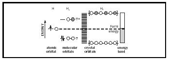
Each band can be filled with electrons in a similar fashion to filling a plastic bottle with sand. If that bottle of sand is completely full, it is possible to tilt it or even turn it upside down and the grains of sand will not move. If the plastic bottle is not completely full (i.e., a partially filled band), then the grains of sand can easily move when the bottle is tilted. They are not localized in one position but delocalized across the top surface. In a similar way, electrons of a partially filled band are delocalized across the crystal and can conduct electricity. The energy of the highest filled levels is called the Fermi energy.
Understanding Conductivity
A metallic conductor is a substance that has a partially filled band. It takes very little energy to move electrons from a filled level to an empty level in a band; this results in high conductivity because there is no energy gap at the Fermi level. When the temperature of a metallic conductor is lowered, the conductivity increases because the thermal motion of the atoms in the crystal is slowed, allowing the electrons to move more easily.
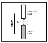
In contrast, both semiconductors and insulators have band structures in which all of their electronic bands are either completely full or completely empty. Because real crystals have more than one orbital, unlike the hydrogen example, there will be several bands giving rise to the electronic band structure. Bands filled with electrons occur below the Fermi energy and bands at higher energy are empty. The difference in energy between the highest part of the filled band and the lowest part of the empty band is the band gap. The difference between an insulator and a semiconductor is the size of the band gap. A material with a band gap of less than about 3.5 eV is considered a semiconductor, whereas materials with larger band gaps are insulators. In a semiconductor, the filled band below the Fermi level is called the valence band and the empty band above the Fermi level is called the conduction band.
If sufficient energy is supplied to a semiconductor, an electron can be promoted from the valence band to the conduction band; this also creates a hole in the valence band. The electron promoted to the conduction band and/or the hole left in the valence band can be delocalized across the crystal, resulting in electronic conductivity. The magnitude of the conductivity is strongly determined by the energy supplied to the semiconductor. For this reason, the conductivity of a semiconductor will increase with increasing temperature.
The Chemistry of Semiconductors
The properties of a semiconductor are determined by the elemental composition of the material, its structure, and the presence of any impurities. Impurities, commonly referred to as dopants, add extrinsic properties to the semiconductor, compared with the properties intrinsic to the pure material itself.
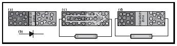
Intrinsic semiconductors. The group fourteen elements carbon, silicon, germanium, and tin can be found to adopt the diamond-type crystal structure shown in Figure 3a. Other crystalline structures are also found; for example, graphite and diamond are different crystal structures of the same element, carbon. Because of its size and orbital energies, carbon forms very
strong bonds, so there is large energy separation between the bonding and antibonding bands in diamond. This results in a large band gap of 6.0 eV, making diamond an insulator. In contrast, bonding between the heavier elements (silicon, germanium, and tin) is not as strong, so the band gap decreases going down the column of the Periodic Table: silicon, 1.1 eV; germanium, 0.7 eV; and grey tin, 0.1 eV. In addition, at temperatures below 13°C (55°F), tin undergoes a crystal rearrangement to the structure of white tin that has no band gap because it is metallic.
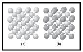
Compound semiconductors are made up of more than one element and give the ability to chemically tune the size of the band gap. Typical compound semiconductors will combine elements from group thirteen and group fifteen on the Periodic Table. These compound semiconductors also adopt a diamond-type crystal structure but with alternation of the atom types in the crystal network (Figure 3b). By combining elements with three and five valence electrons (such as aluminum and phosphorus, respectively)—an average of four electrons per atom—a material with properties similar to silicon with four valence electrons is obtained. However, because the orbitals of phosphorus are lower in energy and the orbitals of aluminum are higher in energy than silicon, a larger band gap is observed for the compound semiconductor AlP (3.0 eV). Combination of the heavier elements gallium and arsenic will form gallium arsenide (GaAs), with a band gap of 1.4 eV. A similar chemistry is possible by combining elements of groups twelve and sixteen, which, for example, yield the semiconductors zinc sulfide (ZnS) and cadmium selenide (CdSe), with band gaps of 3.8 eV and 1.8 eV, respectively.
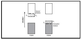
Dopants in semiconductors. Purity for an electronic grade semiconductor must be greater than 99.999 percent. Controlling the amount and type of impurity, however, can fine-tune the properties of the semiconductor. For example, adding a phosphorus impurity (with five valence electrons) to silicon (with four valence electrons) effectively adds one extra electron for each phosphorus atom added to the crystal. Thus the phosphorus is a donor to silicon. The dopant phosphorus atoms will displace silicon atoms in the crystal, but the overall crystal structure does not change, nor does the band structure. The extra electron must go into the conduction band, however, since the valence band was already full. This yields an n -type semiconductor. Conversely, doping silicon with aluminum provides one too few electrons, leaving one hole in the valence band for each aluminum atom added. Thus aluminum is an acceptor from silicon. Having lost electrons, the holes bear a positive charge, forming a p -type semiconductor. Because the gap in energy between the donor levels and the conduction band (E n ) or between the acceptor levels and the valence band (E p ) is very small, these doped semi-conductors will exhibit a greater conductivity and much less temperature dependence than is observed for an intrinsic semiconductor.
The P–N junction. The Fermi level of a p -type semiconductor is lower in energy than that of an n -type semiconductor. When p - and n -type semi-conductors are joined, a common Fermi level is created by the combination of holes and electrons at the interface. No carriers are present in this depletion zone at the junction. When a positive voltage is applied to the p -type side of the p-n junction and a negative voltage to the n -type side, current can flow since the positive voltage pushes the holes toward the
negative cathode and the negative voltage pushes the free electrons toward the positive anode. By contrast, hooking the battery up in reverse will increase the size of the depletion zone, because the negative voltage attached to the p -side of the junction will pull more holes toward that electrode and the positive voltage attached to the n -type semiconductor will pull electrons toward the electrode and away from the junction, leaving a larger depletion zone. As a result there are no free carriers and no current can flow. Thus this p-n junction forms the simplest solid-state device, known as a diode.
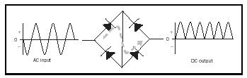
Diodes. Diodes are essentially one-way valves for electronic conductivity. Such a device is very important in a power supply that converts AC to DC current, necessary for many electronic devices. Connecting a single diode to an AC electrical circuit will block either the positive or negative voltage swings, described as half rectification. The connection of four diodes (as shown in Figure 6) will give full wave rectification, converting AC to DC current. The addition of capacitors to this circuit will smooth the voltage oscillations for actual device operation.
When electrical current is passed through any p-n junction, electrons traveling through the conduction band or holes traveling through the valence band can recombine with holes or electrons, respectively, across the band gap. This recombination primarily occurs to electrons that have been pushed into the p -type region of the diode and to holes that have been pushed into the n -type region of the diode by the external voltage. As electrons and holes are recombined across the band gap, energy is released, often as a photon with an energy equal to that of the band gap. Semiconductors with band gaps between 1.8 eV and 3.1 eV will emit photons of visible light (red [700 nanometers; 2.76 × 10 −5 inches] to violet [400 nanometers; 1.58 × 10 −5 inches]). These are known as LEDs. In fact, all diodes emit light, but most have a band gap that is smaller than the energy of a visible photon.
As a result, most diodes emit infrared photons. Such infrared emission is used for signaling in many remote control devices.
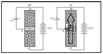
Transistors. Transistors are solid-state switching and amplifying devices, and it was their invention in 1947 that truly began the electronics revolution of the late twentieth century. An n-p-n bipolar transistor is formed by connecting n -type semiconductors on either side of a thin p -type semiconductor. As shown in Figure 7, the transistor acts as a switch for the circuit connected to the 10 V power supply. If a small negative voltage is applied to the base (contact B), the holes are removed from the p -type semiconductor, creating an insulating barrier. This is the same process as trying to force current the wrong way through two p-n junctions. As a result, no current will flow between any of the contacts. If a small positive voltage is applied to the base contact, however, some current will flow through the control loop (electrons going from the emitter to the base). Because the voltage supplied between the emitter (contact E) and the collector (contact C) is much larger than the base voltage, a much greater fraction of the electrons will cross the thin p -type layer, giving the much larger collector current.
As described above, the transistor functions as a simple on/off device, depending on the sign of the voltage applied to across the base and emitter. Because the base current is small and the collector current is large, this same solid-state device can also be used as a signal amplifier. The ratio of the collector current to the base current is essentially constant for a given device. Since the base current is proportional to the base-emitter voltage (voltage between B and E) and the collector current is proportional to the emitter-collector voltage (voltage between E and C), a small oscillation in the voltage input from a microphone, for example, into the BE loop will be
amplified to a large oscillation in the voltage in the EC loop, which then can be connected to a loudspeaker.
Though varying combinations of semiconductors can be fabricated into many different solid-state devices, the operation of the device is strongly dependent on the chemistry of the elements making up the semiconductors. The bonding between elements making up semiconductors determines the electronic band structure and the size of the band gap. The number of valence electrons determines the filling of those bands and thus the electronic properties. Ongoing research efforts continue to discover new semiconductors with new possible applications. In addition, extensive effort is being invested to design smaller and smaller devices with the goal of moving from solid-state devices (based on crystalline materials) to single molecule devices.
James D. Martin
Bibliography
Campbell, Dean J.; Lorenz, Julie K.; Ellis, Arthur B.; Kuech, Thomas F.; Lisensky, George; Whittingham, C.; and Stanley, M. (1998). "The Computer as a Materials Science Benchmark." Journal of Chemical Education 75:297–312.
Ellis, Arthur B.; Geselbracht, Margret J.; Johnson, Brian J.; Lisensky, George C.; and Robinson, William R. (1993). Teaching General Chemistry: A Materials Science Companion. Washington, DC: American Chemical Society.
Internet Resources
"Bell Labs: More Than 50 Years of the Transistor." Lucent Technologies. Available from http://www.lucent.com/minds/transistor .
Brain, Marshall. "How Semiconductors Work." HowStuffWorks, Inc. Available from http://www.howstuffworks.com/diode.htm .
Comment about this article, ask questions, or add new information about this topic: