Semiconductors
The development of semiconductors is clearly among the most significant technological achievements to evolve from the study of solid-state chemistry and physics. Aside from their well-known applications in computers and electronics, semiconductors are also used in a wide variety of optical devices such as lasers, light-emitting diodes, and solar panels. The diversity of applications can be readily understood with only a basic understanding of the theory behind these materials.
Theory
The operation of semiconductors is best understood using band theory. At its most fundamental level, band theory can be extremely complex, requiring relatively advanced mathematics and physics. When a large number of atoms combine to form a solid, the electrons e − in the solid are distributed into energy bands among all the atoms in the solid. Each band has a different energy, and the electrons fill these bands from the lowest energy to the highest, similar to the way electrons occupy the orbitals in a single atom. The variation in properties between electrical insulators, conductors ( metals ), and semiconductors stems from differences in the band structures of these materials (see Figure 1). For this discussion, three terms must be defined. The highest energy band that contains electrons is called the valence band, whereas the lowest energy empty band is called the conduction band. The band gap is the difference in energy between the valence and conduction bands. The laws of quantum mechanics forbid electrons from being in the band gap; thus, an electron must always be in one of the bands.
In a metal (e.g., copper or silver), the valence band is only partially filled with electrons (Figure 1a). This means that the electrons can access empty areas within the valence band, and move freely across all atoms that make up the solid. A current can therefore be generated when a voltage is applied. In general, for electrons to flow in a solid, they must be in a partially filled band or have access to a nearby empty band. In an electrical insulator, there is no possibility for electron flow (Figure 1b), because the valence band is completely filled with electrons, and the conduction band is too far away in energy to be accessed by these electrons (the band gap is too large). A semiconductor (Figure 1c) is a special case in which the band gap is small enough that electrons in the valence band can jump into the conduction band using thermal energy. That is, heat in the material
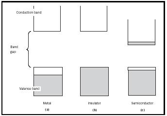
(even at room temperature) gives some of the electrons enough energy to travel across the band gap. Thus, an important property of semiconductors is that their conductivity increases as they are heated up and more electrons fill the conduction band. The most well-known semiconductor is silicon (Si), although germanium (Ge) and gallium arsenide (GaAs) are also common.
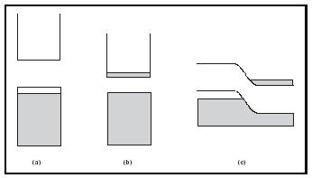
To complete the development of semiconductor theory, the concept of doping must be described (see Figure 2). In principle, the idea is to introduce a different kind of atom into a semiconductor in order to modify its electronic structure. Consider, for example, adding a small amount of phosphorus, P, into a silicon host. Phosphorus is one column to the right of silicon in the Periodic Table, so it contains one additional electron. This means that doping P into Si has the effect of introducing additional electrons to the material, such that some e − must go into the conduction band. Because extra negatively charged electrons are added to the system, phosphorusdoped Si is called an n- type semiconductor, and phosphorus is described as a donor (of electrons). Similarly, a p- type semiconductor can be fabricated by adding an element to the left of Si in the Periodic Table. Boron, B, is a common dopant for a p- type. In this case, the valence band will be missing electrons. These empty locations in a p- type semiconductor are also referred to as holes. Since holes represent the absence of an electron, they carry a positive charge. In p- type semiconductors, boron is referred to as an acceptor (of electrons). From Figure 2, it can be seen that both n- and p- type materials create partially filled bands, allowing for electrical conduction. Dopant concentrations are fairly small, around 10 16 atoms/cm 3 , constituting only about ten-billionths of the total mass of the material.
If p- and n- type materials are layered together, a p-n junction results (Figure 2c). Right at the interface, some of the excess electrons from the n- type combine with holes from the p- type. The resulting charge separation creates an energy barrier that impedes any further movement of electrons. In most technological applications, the important properties of semiconductors are the result of the band structure of the p-n junction. A single
junction based on the same host material (e.g., one interface of p- and n- doped silicon) is called a homojunction. The homojunction model is used here to describe the properties of many devices that are based on semiconductors. However, it should be noted that real systems are typically composed of multiple p-p, n-n, and p-n junctions, called heterojunctions. Such configurations greatly improve the performance of these materials; in fact, the development of heterojunction devices was critical to the widespread practical application of this technology.
Semiconductors in Electronics
Semiconductors are used extensively in solid-state electronic devices and computers. The majority of materials for these applications are based on doped silicon. An important property of p-n junctions is that they allow electron flow only from the n side to the p side. Such one-way devices are called diodes. Consider Figure 2c again. If a positive voltage (also called a forward bias) is applied that lowers the energy barrier between n and p, then the electrons in the conduction band on the n side can flow across the junction (and holes can flow from p to n ). A reverse bias, however, raises the height of the barrier and increases the charge separation at the junction, impeding any flow of electrons from p to n.
Diodes have several important applications in electronics. The power supplied by most electrical utilities is typically alternating current (AC); that is, the direction of current flow switches back and forth with a frequency of sixty cycles per second. However, many electronic devices require a steady flow of current in one direction (direct current or DC). Since a diode only allows current to flow through it in one direction, it can be combined with a capacitor to convert AC input to DC output. For half the AC cycle, the diode passes current and the capacitor is charged up. During the other half of the cycle, the diode blocks any current from the line, but current is provided to the circuit by the capacitor. Diodes applied in this way are referred to as rectifiers.
The by far most important application of semiconductors is as logic gates and transistors in computers. Logic gates, such as OR and AND gates, take advantage of the one-way nature of diodes to compare the presence or
absence of current at different locations in a circuit. More complex solid-state transistors are composed of npn or pnp junctions. The device geometry is slightly more complicated than that observed in a diode, but the result is materials that allow for the generation of the zeros and ones required for the binary logic used by computers.
Optoelectronic Devices
Optoelectronic materials are a special class of semiconductors that can either convert electrical energy into light or absorb light and convert it into electrical energy. Light-emitting diodes (LEDs), for example, are commonly used for information display and in automotive interior lighting applications. In an LED, a forward bias applied across the junction moves electrons in the conduction band over holes in the valence band. The electron and hole combine at the junction, and the energy created by this process is conserved via the emission of light (Figure 3a). The wavelength of emitted light will depend on the band gap of the material; larger band gaps lead to shorter wavelengths of light. Only certain kinds of semiconductors, called direct gap semiconductors, exhibit this behavior. GaAs is an example of a direct gap semiconductor used in these applications. Silicon is an indirect gap material, and electrons and holes combine with the generation of heat instead of light.
A diode laser operates in essentially the same fashion as an LED. Two additional requirements must be met for a direct gap semiconductor to be an efficient laser. The first is that larger forward bias currents are needed for a laser than for an LED, because lasers require a higher degree of population inversion—a large number of electrons in the conduction band above empty levels in the valence band. Lasers also require an optical cavity; light bounces back and forth within the cavity, building up intensity. In a diode

laser, this can be achieved by cleaving and polishing opposite faces of the diode. The smooth faces act like partially reflecting mirrors. This kind of laser is used to read information on compact disks and is also used in laser pointers.
The most common materials for lasers and LEDs are heterojunctions based on GaAs. More complex systems containing Ga, As, P, Al, and N are also used. The band gap of these materials can be tailored to create emission from infrared to yellow. In optical data storage systems, such as compact disks, the amount of information that can be stored is dependent in part on the wavelength of light being used to read the disk—shorter wavelengths allow for denser information storage. Thus, there has been considerable interest in developing larger band gap LEDs and lasers that emit in the blue. This has been achieved in semiconductors based on GaN (gallium nitride). Further refinement of these materials will no doubt lead to significant advances in optoelectronic technology in the coming years.
A final important class of optoelectronic devices based on semiconductors is photovoltaics, such as photodetectors and solar cells. In some respects, these can be regarded as LEDs operating in reverse. Light energy incident on the p-n junction is absorbed by an electron, which then jumps to the conduction band (Figure 3b). Once in the conduction band, the electron travels downhill (energetically) to the n side of the junction, with a hole migrating to the p side. This creates a flow of current that is the reverse of what is seen in a forward biased diode. The result is the conversion of light energy to electrical energy. These devices can therefore be used to detect light, as in digital imaging systems or miniature cameras; or the electrical energy can be stored, as in solar cells. Commercial photovoltaics are based on a variety of host materials, including Si, AlGaAs, and InAlAs.
Fabrication
The industrial fabrication of semiconductors can be extremely complex, involving high-purity materials, sophisticated equipment, and hundreds of steps. Most processes begin with the growth of a large single crystal of n- type Si, called a wafer. A dopant (e.g., phosphorus) is added to high-purity molten silicon, and a crystal is then slowly extracted from this melt. The polished wafer is 20 to 30 centimeters (7.9–11.8 inches) in diameter.
The rest of the processing will depend on the nature of the device being produced. A simple p-n junction is usually fabricated via photolithography and etching processes. In this method, a layer of silicon dioxide, SiO 2 , is created on the surface of the wafer by heating it in the presence of

oxygen. Some of the SiO 2 is then chemically stripped away, or etched, exposing only a portion of the Si wafer. This exposed part of the wafer is made into p- type material by bombarding it with boron ions. As these ions diffuse into the Si wafer, p- type Si is formed. Since the original wafer was n- type, a p-n junction forms where the diffusion of boron stops. Metal contacts can then be added to each side of the junction to create a simple homojunction device.
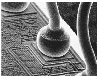
Fabrication of more complicated devices is achieved via combinations of etching, deposition, and ion implantation steps. In the production of integrated circuits for computers, about 400 chips can be synthesized on a single 30-centimeter (11.8-inch) wafer. Each chip may contain as many as 50 million transistors in a space barely more than 1 centimeter (0.39 inches) on a side—a truly remarkable technological achievement. As faster and faster systems are developed, the demand for smaller and smaller features increases. Such miniaturization is the most significant challenge facing the semiconductor industry today.
Semiconductors are used in a wide variety of electronic and optoelectronic applications. The useful properties of semiconductors arise from the unique behavior of doped materials, the special control of electron flow provided by p-n junctions, and the interaction of light energy with electrons at these junctions. The industry continues to grow, and research in this and related areas (i.e., organic semiconductors and molecular transistors) is occurring at academic institutions around the world.
Bibliography
Bhattacharya, Pallab (1994). Semiconductor Optoelectronic Devices . Englewood Cliffs, NJ: Prentice Hall.
May, Gary S., and Sze, Simon M. (2003). Fundamentals of Semiconductor Fabrication. New York: Wiley.
Miessler, Gary L., and Tarr, Donald A. (1999). Inorganic Chemistry , 2nd edition, Upper Saddle River, NJ: Prentice Hall.
Myers, H. P. (1997). Introductory Solid State Physics , 2nd edition. Philadelphia: Taylor & Francis.
Svelto, Orazio (1989). Principles of Lasers , 3rd edition, tr. and ed. David C. Hanna. New York: Plenum.
Texas Instruments Learning Center (1972). Understanding Solid State Electronics , 2nd edition. Dallas: Texas Instruments Inc.
Wold, Aaron, and Dwight, Kirby (1993). Solid State Chemistry . New York: Chapman & Hall.